Fused Quartz & Substrates · TB-SUB-GAN
GaN-on-Sapphire & AlN-on-Sapphire Epi Templates
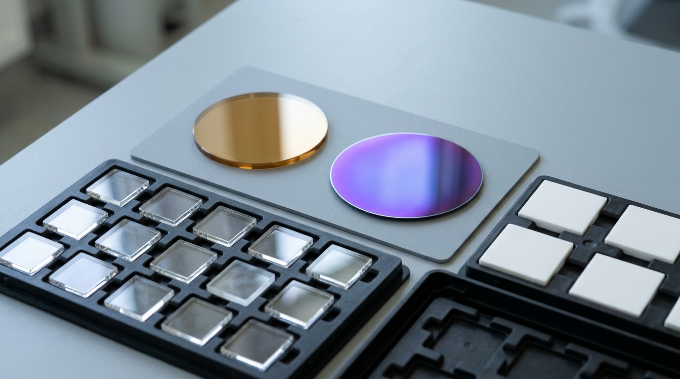
Epi-ready CMP-polished GaN-on-Sapphire & AlN-on-Sapphire epi templates (GaN / AlN on α-Al2O3, CAS 25617-97-4) wafers and diced research squares with sub-nanometer surface roughness for PVD, PLD, MBE, and ALD.
Alternate & search designations: Epi-ready GaN / AlN on α-Al2O3 single crystal wafer, GaN-on-Sapphire & AlN-on-Sapphire epi templates thin-film growth substrate, (0001) C-Plane (1–5 µm AlN or 3–5 µm GaN epilayer on Ø 2" / 4" or 10×10 mm Sapphire) GaN / AlN on α-Al2O3
Purity / Grade OptionsMOCVD / HVPE Epitaxial Template (Undoped, Si-Doped N-Type, or Fe-Doped Semi-Insulating)
Standard Dimensions10×10 mm, 5×5 mm, 10×5 mm, Ø 1", Ø 2", Ø 3", Ø 4" × 0.5 mm / 1.0 mm
Available Configurations1-Side (SSP) or 2-Side (DSP) Epi-Ready CMP Polish; Cleanroom 100 Pack
Ordering & MOQSpecification-based quote · Prototype & production lots
Material & Engineering Overview
Precision-grown and chemical-mechanical-polished (CMP) in a Class 100 cleanroom, our GaN-on-Sapphire & AlN-on-Sapphire epi templates (GaN / AlN on α-Al2O3, CAS 25617-97-4) substrates provide atomically smooth, epi-ready surfaces (Ra < 0.2–0.5 nm) for thin-film epitaxy, pulsed laser deposition (PLD), magnetron sputtering, molecular beam epitaxy (MBE), and optical characterization.
Pre-grown MOCVD/HVPE GaN and AlN epitaxial templates on C-plane sapphire allow labs to jump straight into active III-nitride quantum well, HEMT, UV-LED, and acoustic resonator regrowth or device fabrication. Standard research sizes include 5×5 mm, 10×10 mm, and 15×15 mm diced squares (0.5 mm or 1.0 mm thick) as well as Ø 1-inch, 2-inch, 3-inch, and 4-inch wafers in single-side (SSP) or double-side (DSP) polished finishes, packed in individual waffle trays or nitrogen-sealed cassettes with batch orientation and surface inspection data.
Standard Shipment Documentation: Manufacturer Lot COA (crystal orientation X-ray verification, surface roughness Ra, thickness tolerance, and resistivity/doping if applicable).
Primary Research & Industrial Applications
- AlGaN/GaN HEMT RF & power transistor fabrication and regrowth
- Deep-UV (UVC 230–280 nm) LED and solar-blind photodetector epitaxy on AlN/Sapphire templates
- GaN photonic crystals, micro-LED arrays, and polariton cavity devices
- High-frequency SAW/BAW acoustic wave devices on single-crystal AlN/Sapphire
Nominal Material Reference Properties
| Property / Metric | Nominal Reference Value (Grade Dependent) |
|---|
| Formula & CAS # | GaN / AlN on α-Al2O3 (CAS 25617-97-4) |
| Crystal System / Grade | Hexagonal Wurtzite (0001) on C-Plane Sapphire · MOCVD / HVPE Epitaxial Template (Undoped, Si-Doped N-Type, or Fe-Doped Semi-Insulating) |
| Density | 6.15 (GaN) / 3.26 (AlN) g/cm³ |
| Standard Orientations | (0001) C-Plane (1–5 µm AlN or 3–5 µm GaN epilayer on Ø 2" / 4" or 10×10 mm Sapphire) |
| Surface Finish (CMP) | Epi-Ready As-Grown Atomic Step Surface (Ra < 0.3 nm) |
Reference values reflect typical sintered, fused, or wrought grades. Exact batch test figures are confirmed on your written quotation and accompanying lot Certificate of Analysis.
What to Specify in Your Quote Request
Specify GaN / AlN on α-Al2O3 crystallographic orientation ((0001) C-Plane (1–5 µm AlN or 3–5 µm GaN epilayer on Ø 2" / 4" or 10×10 mm Sapphire)), dimensions and thickness (e.g., 10×10×0.5 mm or Ø 2" × 0.5 mm), SSP vs. DSP polish, edge orientation, and pack count.
Include target quantity, destination country/postal code for express air freight calculation, and any special cleanroom bagging or certification requests.
Prepare GaN-on-Sapphire & AlN-on-Sapphire Epi Templates RFQ ↗
Technical & Procurement FAQ
Are GaN-on-Sapphire & AlN-on-Sapphire epi templates (GaN / AlN on α-Al2O3) substrates ready for epitaxial deposition out of the box?
Yes. All epi-ready substrates are final CMP-polished and packaged in cleanroom waffle packs or sealed containers with sub-nanometer Ra roughness.
What tolerances apply to 10×10×0.5 mm diced GaN / AlN on α-Al2O3 substrates?
Standard lateral dimensions are ±0.05–0.10 mm, thickness is ±0.02–0.05 mm, and crystal axis orientation accuracy is within ±0.5° (or ±0.1° on custom request).
Can I order custom sizes, thicknesses, or double-side polishing for TB-SUB-GAN?
Yes. Both single-side (SSP) and double-side (DSP) polished substrates as well as custom laser/wire-saw diced dimensions can be quoted with no high minimum order quantity.
 TB-SAP-SB