TB-SIO2-TUHigh-Purity Fused Quartz Furnace Tubes
Optically clear 99.99% (4N) fused quartz process tubes for CVD graphene/2D growth, semiconductor diffusion, photochemistry, and rapid-quench tube furnaces up to 1,150 °C.
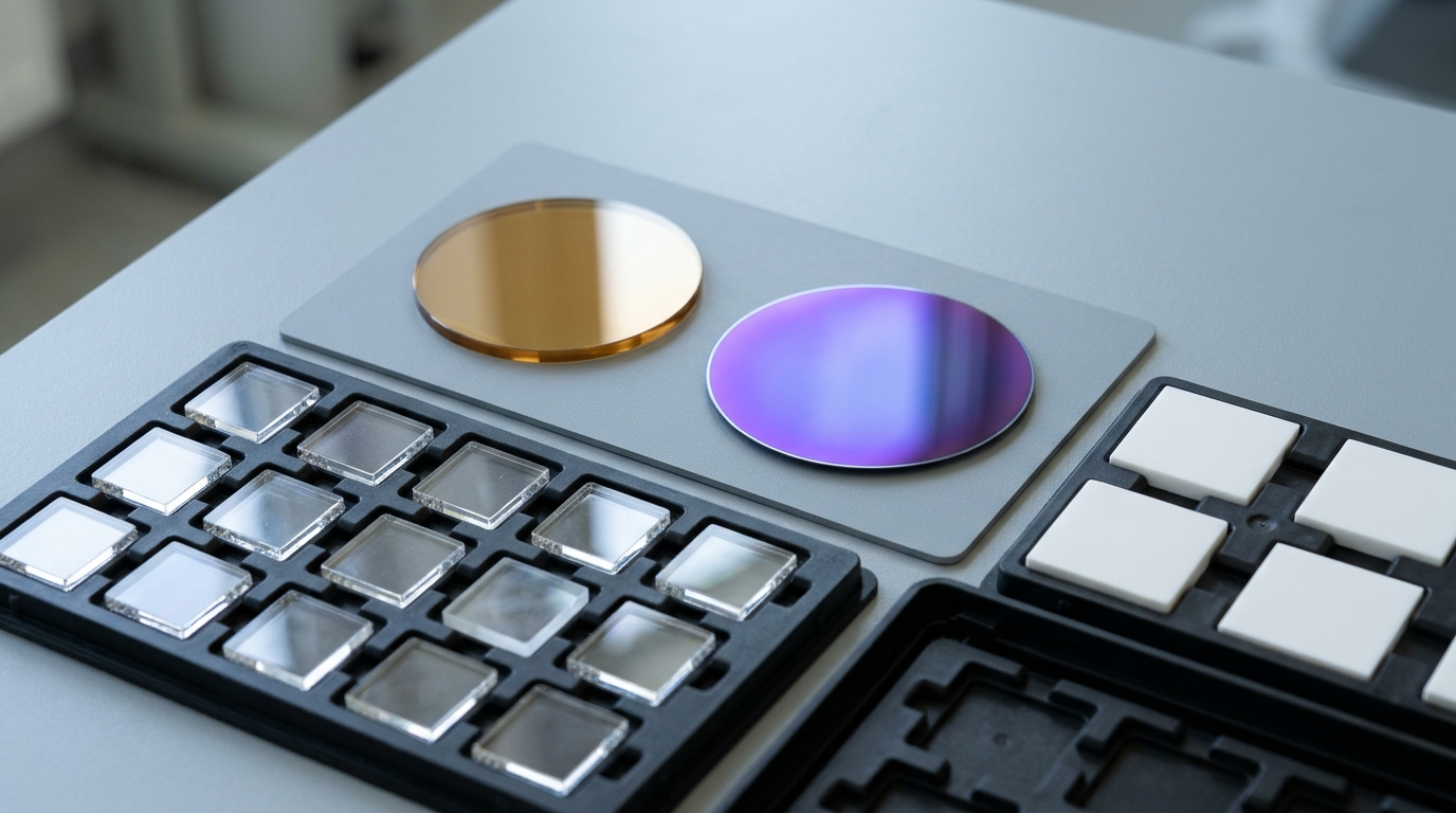
Semiconductor- and laboratory-grade 99.99% fused quartz process tubes, slotted wafer boats, crucibles, UV-grade fused silica optical windows, and single-crystal C-plane sapphire substrates for CVD, diffusion, photonics, and spectroscopy.

Compare SKU codes, chemical formulas, CAS numbers, purity grades, and standard dimensional envelopes.
| SKU | Product Line | Formula | CAS # | Purity / Grade | Typical Dimensions | RFQ |
|---|---|---|---|---|---|---|
| TB-SIO2-TU | High-Purity Fused Quartz Furnace Tubes | SiO2 | 60676-86-0 | ≥99.99% SiO2 (4N Semiconductor Grade, <20 ppm total metals) | OD 6–300 mm × Wall 1.5–8 mm × Length up to 2,000 mm | Quote ↗ |
| TB-SIO2-BT | Fused Quartz Sample Boats & Wafer Carriers | SiO2 | 60676-86-0 | ≥99.99% SiO2 Semiconductor-Grade Quartz | Boats 30–300 mm; Slotted carriers for 10×10 mm chips up to 8-inch wafers | Quote ↗ |
| TB-SIO2-CR | Clear Fused Quartz Crucibles & Evaporating Dishes | SiO2 | 60676-86-0 | ≥99.99% SiO2 Clear Fused Quartz | 10 mL to 1,000 mL crucibles, beakers, & flat dishes | Quote ↗ |
| TB-SIO2-WN | UV Fused Silica & Optical Quartz Windows | SiO2 | 60676-86-0 | JGS1 (Deep-UV 185–2,100 nm) / JGS2 (UV-VIS) / JGS3 (IR Low-OH) | Ø 5–200 mm or Square 5×5 to 150×150 mm × Thickness 0.2–20 mm | Quote ↗ |
| TB-SAP-SB | Single-Crystal Sapphire Windows & Substrates | α-Al2O3 (Single Crystal) | 1344-28-1 | ≥99.995% Single-Crystal Al2O3 (4N5–5N Kyropoulos/EFG) | Chips 5×5, 10×10 mm; Windows Ø 5–100 mm; Wafers 2", 4", 6" | Quote ↗ |
| TB-SUB-SI | Silicon Wafers & Thermal Oxide (SiO2/Si) Substrates | Si / SiO2-on-Si | 7440-21-3 | Prime / Test CZ & FZ Grade (1–100 Ω·cm, Intrinsic >5,000 Ω·cm, or Degenerate 0.001–0.005 Ω·cm) | 10×10 mm, 5×5 mm, 10×5 mm, Ø 1", Ø 2", Ø 3", Ø 4" × 0.5 mm / 1.0 mm | Quote ↗ |
| TB-SUB-SIC | Single-Crystal 4H-SiC & 6H-SiC Wafers & Substrates | SiC (4H / 6H) | 409-21-2 | PVT Single-Crystal N-Type Conductive & High-Purity Semi-Insulating (HPSI) | 10×10 mm, 5×5 mm, 10×5 mm, Ø 1", Ø 2", Ø 3", Ø 4" × 0.5 mm / 1.0 mm | Quote ↗ |
| TB-SUB-MGO | Magnesium Oxide (MgO) Single-Crystal Substrates | MgO | 1309-48-4 | Arc-Fusion Single Crystal 4N (99.99%) | 10×10 mm, 5×5 mm, 10×5 mm, Ø 1", Ø 2", Ø 3", Ø 4" × 0.5 mm / 1.0 mm | Quote ↗ |
| TB-SUB-STO | Strontium Titanate (SrTiO3 & Nb:STO) Single-Crystal Substrates | SrTiO3 / Nb:SrTiO3 | 12060-59-2 | Verneuil Single Crystal 4N (Undoped Insulating or 0.05–0.7 wt% Nb-Doped Conductive) | 10×10 mm, 5×5 mm, 10×5 mm, Ø 1", Ø 2", Ø 3", Ø 4" × 0.5 mm / 1.0 mm | Quote ↗ |
| TB-SUB-LAO | Lanthanum Aluminate (LaAlO3) Single-Crystal Substrates | LaAlO3 | 12003-65-5 | Czochralski Single Crystal 4N (99.99%) | 10×10 mm, 5×5 mm, 10×5 mm, Ø 1", Ø 2", Ø 3", Ø 4" × 0.5 mm / 1.0 mm | Quote ↗ |
| TB-SUB-YSZ | Yttria-Stabilized Zirconia (YSZ) Single-Crystal Substrates | ZrO2:Y2O3 (8–9.5 mol% Y2O3) | 1314-23-4 | Skull-Melted Cubic Single Crystal 4N | 10×10 mm, 5×5 mm, 10×5 mm, Ø 1", Ø 2", Ø 3", Ø 4" × 0.5 mm / 1.0 mm | Quote ↗ |
| TB-SUB-LNO | Lithium Niobate (LiNbO3) & Lithium Tantalate (LiTaO3) Wafers | LiNbO3 / LiTaO3 | 12031-63-9 | Czochralski Optical / SAW / Black-Reduced Grade (Congruent, Stoichiometric, or 5 mol% MgO-Doped) | 10×10 mm, 5×5 mm, 10×5 mm, Ø 1", Ø 2", Ø 3", Ø 4" × 0.5 mm / 1.0 mm | Quote ↗ |
| TB-SUB-GAN | GaN-on-Sapphire & AlN-on-Sapphire Epi Templates | GaN / AlN on α-Al2O3 | 25617-97-4 | MOCVD / HVPE Epitaxial Template (Undoped, Si-Doped N-Type, or Fe-Doped Semi-Insulating) | 10×10 mm, 5×5 mm, 10×5 mm, Ø 1", Ø 2", Ø 3", Ø 4" × 0.5 mm / 1.0 mm | Quote ↗ |
| TB-SUB-SPN | Magnesium Aluminate Spinel (MgAl2O4) Substrates & Windows | MgAl2O4 | 1306-44-1 | Czochralski Single Crystal 4N (99.99%) | 10×10 mm, 5×5 mm, 10×5 mm, Ø 1", Ø 2", Ø 3", Ø 4" × 0.5 mm / 1.0 mm | Quote ↗ |
| TB-SUB-QZC | Single-Crystal Quartz (AT-Cut, ST-Cut, X/Y/Z-Cut) Substrates & Windows | α-SiO2 (Single Crystal) | 14808-60-7 | Hydrothermal Cultured Electronic & Optical Grade Single Crystal | 10×10 mm, 5×5 mm, 10×5 mm, Ø 1", Ø 2", Ø 3", Ø 4" × 0.5 mm / 1.0 mm | Quote ↗ |
| TB-SUB-CAF2 | CaF2, BaF2 & MgF2 UV / Infrared Crystal Windows & Substrates | CaF2 / BaF2 / MgF2 | 7789-75-5 | Vacuum Bridgman Single-Crystal UV / VUV / IR Excimer Grade | 10×10 mm, 5×5 mm, 10×5 mm, Ø 1", Ø 2", Ø 3", Ø 4" × 0.5 mm / 1.0 mm | Quote ↗ |
| TB-SUB-GLS | Borosilicate (Borofloat 33), Alkali-Free Display & FTO/ITO Glass Substrates | SiO2-B2O3-Al2O3 / ITO-Glass / FTO-Glass | 65997-17-3 | Schott Borofloat 33, Alkali-Free Display Glass, & Pre-Coated ITO/FTO Research Slides | 10×10 mm, 5×5 mm, 10×5 mm, Ø 1", Ø 2", Ø 3", Ø 4" × 0.5 mm / 1.0 mm | Quote ↗ |
| TB-SIO2-BK | Semiconductor Fused Quartz Beakers, Wet-Bench Tanks & Vacuum Bell Jars | SiO2 (99.995%) | 60676-86-0 | 99.995% Semiconductor & Trace-Metal Analytical Grade | Beakers 25 mL to 5,000 mL; Rectangular RCA Wet-Bench Tanks; Flanged Quartz Bell Jars | Quote ↗ |
| TB-SIO2-CV | UV-VIS-NIR Fused Quartz Spectrophotometer & Fluorometer Cuvettes (190–2,500 nm) | SiO2 (JGS1 / JGS2 / JGS3) | 60676-86-0 | JGS1 Synthetic Far-UV Quartz (190–2,500 nm) & JGS3 IR Quartz (260–3,500 nm) | Path Lengths: 1 mm, 2 mm, 5 mm, 10 mm, 20 mm, 50 mm, 100 mm (Standard 12.5×12.5×45 mm OD) | Quote ↗ |
| TB-SIO2-FR | Sintered Porous Quartz Fritted Discs, Precision Quartz Rods & Micro-Capillaries | SiO2 (99.99%) | 60676-86-0 | 99.99% Fused Quartz (Porous Grades G00/G0/G1/G2/G3/G4/G5 & Solid/Capillary) | Frits Ø 4–150 mm × 1.5–6 mm; Solid Rods Ø 1–60 mm; Capillaries ID 0.1–4 mm | Quote ↗ |
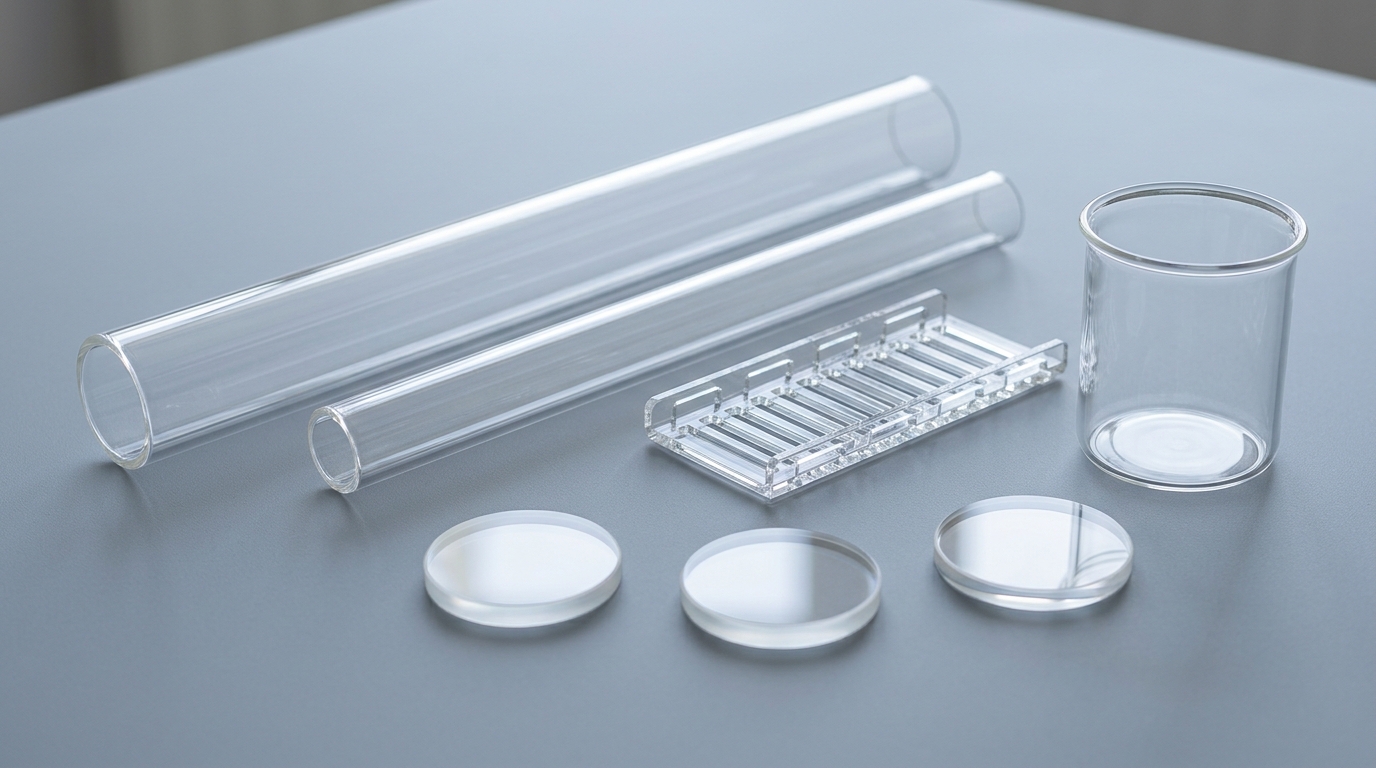
TB-SIO2-TUOptically clear 99.99% (4N) fused quartz process tubes for CVD graphene/2D growth, semiconductor diffusion, photochemistry, and rapid-quench tube furnaces up to 1,150 °C.
TB-SIO2-BTUltra-clean 99.99% fused quartz combustion boats, lidded CVD precursor sleds, and precision-slotted wafer carriers for contamination-free thermal processing.
TB-SIO2-CRFlame-polished 99.99% clear fused quartz crucibles, lids, and evaporating dishes for ultra-trace acid digestion, phosphor firing, and thermal shock cycling.
TB-SIO2-WNPrecision double-side optically polished UV synthetic fused silica (JGS1), optical quartz (JGS2), and full-spectrum IR fused silica (JGS3) windows and wafer substrates.
TB-SAP-SBEpi-ready single-crystal sapphire substrates (C-, R-, A-, M-plane) and Mohs-9 optical sapphire pressure/IR windows from 180 nm UV to 5.0 µm mid-IR.
TB-SUB-SIEpi-ready CMP-polished silicon wafers & thermal oxide (SiO2/Si) substrates (Si / SiO2-on-Si, CAS 7440-21-3) wafers and diced research squares with sub-nanometer surface roughness for PVD, PLD, MBE, and ALD.
TB-SUB-SICEpi-ready CMP-polished Single-Crystal 4H-SiC & 6H-SiC wafers & substrates (SiC (4H / 6H), CAS 409-21-2) wafers and diced research squares with sub-nanometer surface roughness for PVD, PLD, MBE, and ALD.
TB-SUB-MGOEpi-ready CMP-polished magnesium oxide (MgO) Single-Crystal substrates (MgO, CAS 1309-48-4) wafers and diced research squares with sub-nanometer surface roughness for PVD, PLD, MBE, and ALD.
TB-SUB-STOEpi-ready CMP-polished strontium titanate (SrTiO3 & Nb:STO) Single-Crystal substrates (SrTiO3 / Nb:SrTiO3, CAS 12060-59-2) wafers and diced research squares with sub-nanometer surface roughness for PVD, PLD, MBE, and ALD.
TB-SUB-LAOEpi-ready CMP-polished lanthanum aluminate (LaAlO3) Single-Crystal substrates (LaAlO3, CAS 12003-65-5) wafers and diced research squares with sub-nanometer surface roughness for PVD, PLD, MBE, and ALD.
TB-SUB-YSZEpi-ready CMP-polished Yttria-Stabilized zirconia (YSZ) Single-Crystal substrates (ZrO2:Y2O3 (8–9.5 mol% Y2O3), CAS 1314-23-4) wafers and diced research squares with sub-nanometer surface roughness for PVD, PLD, MBE, and ALD.
TB-SUB-LNOEpi-ready CMP-polished lithium niobate (LiNbO3) & lithium tantalate (LiTaO3) wafers (LiNbO3 / LiTaO3, CAS 12031-63-9) wafers and diced research squares with sub-nanometer surface roughness for PVD, PLD, MBE, and ALD.
TB-SUB-GANEpi-ready CMP-polished GaN-on-Sapphire & AlN-on-Sapphire epi templates (GaN / AlN on α-Al2O3, CAS 25617-97-4) wafers and diced research squares with sub-nanometer surface roughness for PVD, PLD, MBE, and ALD.
TB-SUB-SPNEpi-ready CMP-polished magnesium aluminate spinel (MgAl2O4) substrates & windows (MgAl2O4, CAS 1306-44-1) wafers and diced research squares with sub-nanometer surface roughness for PVD, PLD, MBE, and ALD.
TB-SUB-QZCEpi-ready CMP-polished Single-Crystal quartz (AT-Cut, ST-Cut, X/Y/Z-Cut) substrates & windows (α-SiO2 (Single Crystal), CAS 14808-60-7) wafers and diced research squares with sub-nanometer surface roughness for PVD, PLD, MBE, and ALD.
TB-SUB-CAF2Epi-ready CMP-polished CaF2, BaF2 & MgF2 UV / infrared crystal windows & substrates (CaF2 / BaF2 / MgF2, CAS 7789-75-5) wafers and diced research squares with sub-nanometer surface roughness for PVD, PLD, MBE, and ALD.
TB-SUB-GLSEpi-ready CMP-polished borosilicate (borofloat 33), Alkali-Free display & FTO/ITO glass substrates (SiO2-B2O3-Al2O3 / ITO-Glass / FTO-Glass, CAS 65997-17-3) wafers and diced research squares with sub-nanometer surface roughness for PVD, PLD, MBE, and ALD.
TB-SIO2-BKSemiconductor-grade 99.995% clear fused quartz beakers, rectangular wafer wet-bench tanks, and flanged vacuum bell jars with sub-ppm metallic leaching and extreme thermal-shock immunity.
TB-SIO2-CVDirect thermally fused (adhesive-free) JGS1 UV-VIS-NIR quartz spectrophotometer and fluorometer cuvettes with >80% transmission from 190 nm to 2,500 nm and matched pair transmission within ≤0.5%.
TB-SIO2-FRSintered porous fused quartz fritted discs (porosities G0–G5, 2–250 µm), precision centerless-ground quartz rods, and micro-capillary tubing for plug-flow catalyst reactors and gas sparging.
Submit your purity grade, geometry, quantity, and documentation requirements. Every order includes the producing mill's batch Certificate of Analysis (COA) and pre-shipment dimensional verification.