Fused Quartz & Substrates · TB-SAP-SB
Single-Crystal Sapphire Windows & Substrates
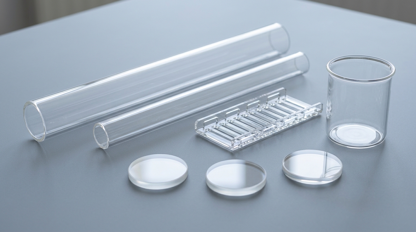
Epi-ready single-crystal sapphire substrates (C-, R-, A-, M-plane) and Mohs-9 optical sapphire pressure/IR windows from 180 nm UV to 5.0 µm mid-IR.
Alternate & search designations: C-plane (0001) epi-ready sapphire wafer, synthetic corundum high-pressure viewport, optical Al2O3 scratch-proof window, GaN/AlN growth substrate
Purity / Grade Options≥99.995% Single-Crystal Al2O3 (4N5–5N Kyropoulos/EFG)
Standard DimensionsChips 5×5, 10×10 mm; Windows Ø 5–100 mm; Wafers 2", 4", 6"
Available ConfigurationsC-plane (0001), A-plane, R-plane, M-plane; SSP or DSP epi-ready
Ordering & MOQSpecification-based quote · Prototype & production lots
Material & Engineering Overview
Single-crystal alpha-Al2O3 (synthetic sapphire, Mohs hardness 9—second only to diamond and SiC/cBN) combines extreme mechanical strength and chemical inertness with broad optical transmission spanning UV (180 nm) through visible to mid-infrared (5.0 µm). In thin-film epitaxy and PVD research, epi-polished C-plane (0001), R-plane (1-102), and A-plane (11-20) substrates serve as the foundational lattice template for GaN, AlN, ZnO, superconducting YBCO, and 2D transition-metal dichalcogenide growth.
Available in pre-diced cleanroom research packs (5×5, 10×10, 10×15 mm), SEMI-standard 2"/4" wafers (single- or double-side epi-polished), and thick optical sight windows.
Standard Shipment Documentation: Manufacturer Lot Crystal COA (crystal orientation X-ray off-cut tolerance, Ra roughness, thickness/TTV, scratch-dig) in Class-100 cleanroom single/pack cases.
Primary Research & Industrial Applications
- Epitaxial & PVD thin-film growth (GaN, AlN, ZnO, graphene, MoS2, oxides)
- High-pressure, subsea, and abrasive-environment optical viewports & IR domes
- Mid-IR spectroscopy (3–5 µm thermal imaging) and high-temperature furnace sight ports
- Precision ruby/sapphire orifice nozzles and ultra-hard bearing flats
Nominal Material Reference Properties
| Property / Metric | Nominal Reference Value (Grade Dependent) |
|---|
| Purity & Structure | ≥99.995% monocrystalline trigonal α-Al2O3 |
| Transmission Band | 180 nm – 5,000 nm (>83–85% uncoated across VIS-MWIR) |
| Mohs / Knoop Hardness | Mohs 9 (~2,000 kg/mm² Knoop) |
| Epi Surface Roughness | Ra < 0.2–0.3 nm (CMP epi-ready finish) |
| Melting Point | 2,040–2,053 °C (usable optically past 1,500 °C) |
Reference values reflect typical sintered, fused, or wrought grades. Exact batch test figures are confirmed on your written quotation and accompanying lot Certificate of Analysis.
What to Specify in Your Quote Request
For substrates, specify crystal orientation (C-, R-, A-, M-, or random optical), chip/wafer size, thickness (e.g., 0.43, 0.50, or 1.0 mm), SSP vs. DSP epi-polish, and SEMI flat. For optical windows, specify diameter × thickness, C-axis zero-birefringence orientation if polarization-sensitive, and scratch-dig.
Include target quantity, destination country/postal code for express air freight calculation, and any special cleanroom bagging or certification requests.
Prepare Single-Crystal Sapphire Windows & Substrates RFQ ↗
Technical & Procurement FAQ
What is the difference between SSP and DSP epi-ready sapphire substrates?
SSP (Single-Side Polished) has one CMP epi-ready growth surface (Ra <0.2 nm) and a fine-ground backside (Ra ~0.8–1.2 µm) conducive to radiative heater coupling, whereas DSP (Double-Side Polished) is optically transparent through both faces for transmission spectroscopy.
Why specify C-axis (0001) orientation on optical sapphire windows?
Sapphire is weakly birefringent along random axes; cutting windows perpendicular to the optical C-axis (0001) minimizes birefringence along the normal beam path.
Are 10×10 mm diced sapphire substrates supplied individually packed?
Yes—diced research substrates ship in cleanroom waffle packs or individual wafer trays (typically packs of 5, 10, or 25 substrates) ready for direct chamber loading.
 TB-SIO2-WN