Fused Quartz & Substrates · TB-SIO2-WN
UV Fused Silica & Optical Quartz Windows
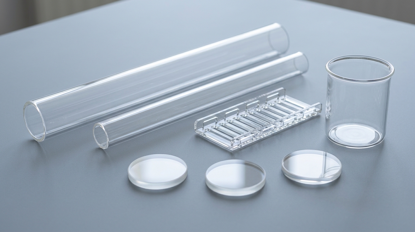
Precision double-side optically polished UV synthetic fused silica (JGS1), optical quartz (JGS2), and full-spectrum IR fused silica (JGS3) windows and wafer substrates.
Alternate & search designations: JGS1 synthetic UV fused silica window, JGS3 IR quartz disc, laser protective viewport blank, double-side polished fused silica wafer
Purity / Grade OptionsJGS1 (Deep-UV 185–2,100 nm) / JGS2 (UV-VIS) / JGS3 (IR Low-OH)
Standard DimensionsØ 5–200 mm or Square 5×5 to 150×150 mm × Thickness 0.2–20 mm
Available ConfigurationsDouble-side optical polish (60/40, 40/20, 20/10), AR coatings, stepped viewports
Ordering & MOQSpecification-based quote · Prototype & production lots
Material & Engineering Overview
Optical-grade fused silica windows combine wide spectral transmission (from 185 nm deep-UV in synthetic JGS1 out to 3,500 nm mid-IR in anhydrous JGS3) with high laser-induced damage thresholds, vacuum viewport strength, and near-zero thermal lensing. Pitch-polished on both faces with protective edge bevels, these windows and thin wafer substrates serve spectroscopy cells, fiber/excimer laser protective heads, PVD optical monitoring ports, and MEMS/microfluidics fabrication.
Custom diameters, square/rectangular plates, drilled apertures, wedge angles, and anti-reflective (AR) coatings are quoted to optical print.
Standard Shipment Documentation: Manufacturer Lot Optical/Material COA (grade, transmission curve spec, scratch-dig & dimensional inspection); cleanroom single-wafer/tray packaging.
Primary Research & Industrial Applications
- Deep-UV (193/248/266 nm) to NIR (1,064 nm) laser optics & protective debris windows
- Vacuum chamber sight glasses, furnace pyrometer viewports, and spectroscopy cuvettes
- Double-side polished 2", 3", 4", and 6" fused silica MEMS & photonics wafers
- Photolithography photomask blanks and microfluidic device bonding
Nominal Material Reference Properties
| Property / Metric | Nominal Reference Value (Grade Dependent) |
|---|
| Optical Grades | JGS1 (185–2,100 nm, >90% UV), JGS2 (220–2,500 nm), JGS3 (260–3,500 nm) |
| Refractive Index (nd) | 1.4585 at 587.6 nm |
| Surface Quality | 60/40 standard; 40/20 or 20/10 laser-grade scratch-dig |
| Flatness / Parallelism | λ/4 to λ/10 flatness; ≤1–3 arcmin (or <10 arcsec precision) |
| Surface Roughness | Ra < 0.5–1.0 nm optical polish |
Reference values reflect typical sintered, fused, or wrought grades. Exact batch test figures are confirmed on your written quotation and accompanying lot Certificate of Analysis.
What to Specify in Your Quote Request
Specify optical grade (JGS1 synthetic UV, JGS2 general optical/viewport, or JGS3 IR low-OH), diameter or L×W, thickness, scratch-dig surface quality, transmitted wavefront/flatness, parallelism, and any AR coating wavelength.
Include target quantity, destination country/postal code for express air freight calculation, and any special cleanroom bagging or certification requests.
Prepare UV Fused Silica & Optical Quartz Windows RFQ ↗
Technical & Procurement FAQ
Which fused silica grade should I select: JGS1, JGS2, or JGS3?
Choose JGS1 (synthetic CVD fused silica, equivalent to Corning 7980 / Suprasil class) for deep-UV transmission down to 185 nm and zero fluorescence; JGS2 for economical visible/1,064 nm viewports and wafers; and JGS3 where 2.7 µm OH absorption bands must be eliminated in the infrared.
Are thin 0.5 mm and 1.0 mm fused silica wafers shipped in cleanroom coin-style or cassette packs?
Yes—polished wafers and optical windows are individually packed in cleanroom single-wafer containers, gel-paks, or lint-free lens tissue sleeves.
Can windows be fabricated with stepped shoulders for pressure or vacuum O-ring viewports?
Yes—stepped, beveled, and thick pressure-rated sight-glass blanks are CNC ground and optically polished to drawing.
 TB-SAP-SB