Thin Film Materials · TB-PVD-SIC
Silicon Carbide (SiC) Sputtering Targets
High-density hot-pressed silicon carbide (SiC, CAS 409-21-2) ceramic sputtering targets in 4N (99.99%) / 4N5 purity, indium-bonded for arc-free RF and pulsed-DC thin-film deposition.
Alternate & search designations: Silicon Carbide RF magnetron target, SiC PVD dielectric cathode disc, 4N sintered SiC RF & conductive pulsed-DC sputtering target
Purity / Grade Options4N (99.99%) / 4N5
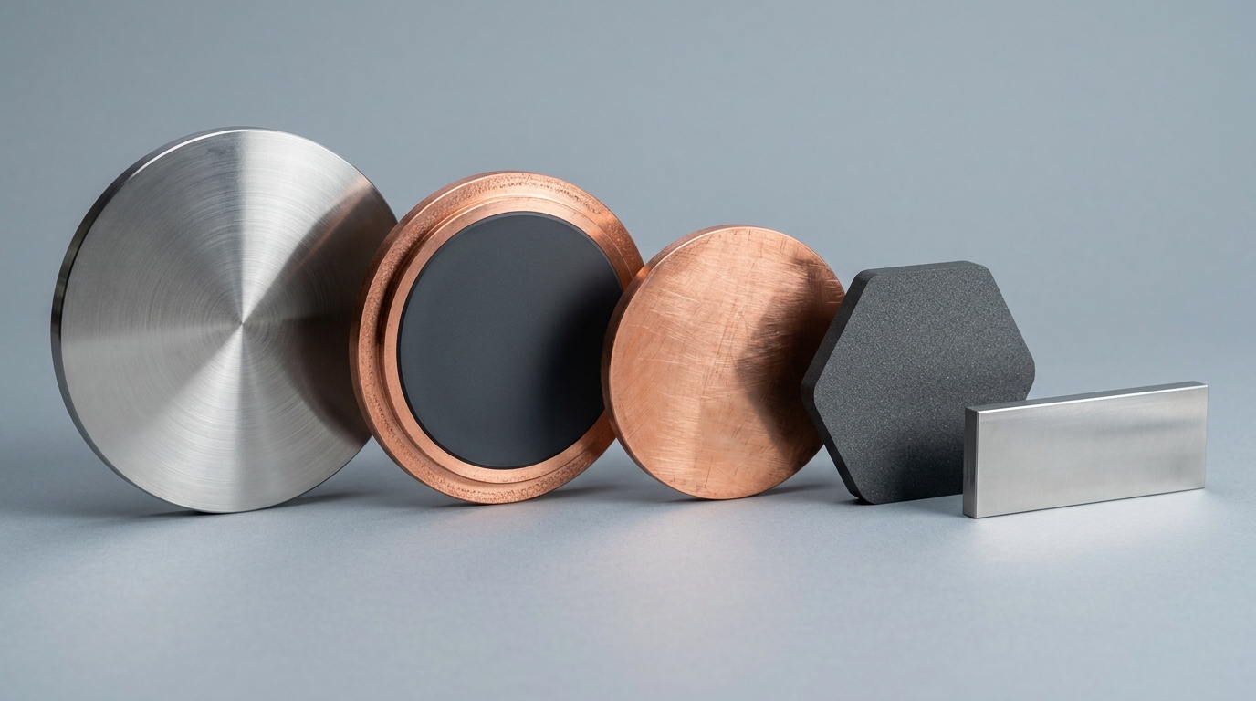
Standard DimensionsØ 1", 2", 3", 4", 6" × Thickness 2–6.35 mm (+ OFHC Cu Backing Plate)
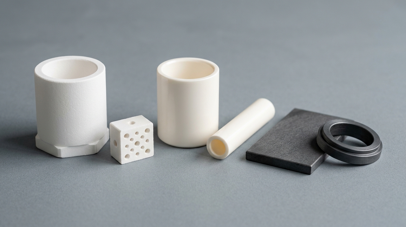
Available ConfigurationsHot-pressed / HIP high-density ceramic disc; Metallic Indium bonded to OFHC Cu
Ordering & MOQSpecification-based quote · Prototype & production lots
Material & Engineering Overview
Sintered by vacuum hot-pressing or Hot Isostatic Pressing (HIP) from sub-micron 4N (99.99%) / 4N5 precursor powders, our silicon carbide (SiC, CAS 409-21-2) sputtering targets achieve high relative density (typically 96%–99.5% of 3.14 g/cm³ theoretical density) and homogeneous phase stoichiometry. High density suppresses outgassing, surface nodule formation, and plasma arcing during RF magnetron or reactive pulsed-DC sputtering.
Available in direct-sintered RF grade and conductive nitrogen-doped / hot-pressed grades for pulsed-DC and RF deposition of ultra-hard wide-bandgap SiC films. Because ceramic targets have low thermal conductivity and limited thermal-shock resistance, we strongly recommend ordering SiC targets metallic-indium bonded to an OFHC copper backing plate. Each target ships vacuum-packed with its batch chemical assay and density COA.
Standard Shipment Documentation: Manufacturer Lot COA (stoichiometry, trace metal ICP assay in ppm, sintered bulk density) and backing-plate bond inspection.
Primary Research & Industrial Applications
- Extreme-UV (EUV) and synchrotron X-ray reflective mirror coatings
- Harsh-environment MEMS pressure/temperature sensor passivation
- Hard tribological diamond-like / SiC wear protection coatings
- Wide-bandgap optoelectronic and power device buffer layers
Nominal Material Reference Properties
| Property / Metric | Nominal Reference Value (Grade Dependent) |
|---|
| Formula & CAS # | SiC (CAS 409-21-2) |
| Purity Grades | 4N (99.99%) / 4N5 |
| Bulk / Theoretical Density | 3.14 g/cm³ (≥96%–99.5% relative density) |
| Recommended Bonding | Metallic Indium bond to OFHC Cu backing plate (<120 °C max run temp) |
| Recommended Power Ramp | RF / Pulsed-DC ramp at 5–10 W/min with ≥2–4 L/min cooling water |
Reference values reflect typical sintered, fused, or wrought grades. Exact batch test figures are confirmed on your written quotation and accompanying lot Certificate of Analysis.
What to Specify in Your Quote Request
Specify SiC purity (4N (99.99%) / 4N5), exact dopant weight/mole ratio if applicable, ceramic disc diameter × thickness (e.g., Ø 50.8 × 3.175 mm), backing-plate geometry, and sputtering chamber gun model.
Include target quantity, destination country/postal code for express air freight calculation, and any special cleanroom bagging or certification requests.
Prepare Silicon Carbide (SiC) Sputtering Targets RFQ ↗
Technical & Procurement FAQ
Why should silicon carbide (SiC) targets be indium-bonded to an OFHC copper backing plate?
As a brittle ceramic, SiC develops steep radial thermal gradients under RF plasma heating; full-coverage metallic indium bonding transfers heat efficiently into the water-cooled copper backing plate and prevents thermal-stress cracking.
What RF power conditioning procedure avoids cracking a new SiC target?
Start at low RF power (~15–25 W on a 2-inch target), ramp slowly at 5–10 W/min over 20–30 minutes while monitoring reflected power, and never exceed ~2–4 W/cm² power density on dielectric oxide/nitride targets.
Is oxygen or nitrogen reactive gas backfill needed when sputtering SiC?
RF sputtering in pure argon often produces slightly anion-deficient films; introducing 1%–10% O2 (for oxides) or N2 (for nitrides) in the Ar plasma restores full stoichiometry and optical transparency.
 TB-PVD-OX