Thin Film Materials · TB-PVD-TE
Tellurium (Te) Sputtering Targets
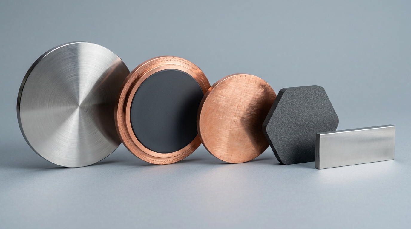
Vacuum-melted high-purity tellurium (Te, CAS 13494-80-9) planar magnetron sputtering targets in 4N (99.99%) / 4N5 / 5N (99.999%) grades for semiconductor, optical, and research PVD.
Alternate & search designations: High-purity tellurium PVD magnetron target, 4N (99.99%) / 4N5 / 5N (99.999%) Te planar sputter cathode disc, 5N tellurium chalcogenide PVD target, indium-bonded Te sputter disc
Purity / Grade Options4N (99.99%) / 4N5 / 5N (99.999%)
Standard DimensionsØ 1", 2", 3", 4", 6", 8" × Thickness 2–12.7 mm; Rectangular
Available ConfigurationsMonolithic or OFHC Cu / Mo backing plate + Metallic Indium / Elastomer bonding
Ordering & MOQSpecification-based quote · Prototype & production lots
Material & Engineering Overview
High-purity tellurium (Te, CAS 13494-80-9) planar sputtering targets are consolidated by vacuum melting or hot isostatic pressing and thermomechanically processed to achieve fine, equiaxed microstructure and ≥99.5%–100% relative density. Controlled grain uniformity and ultra-low dissolved gas content (O, N, H, C) ensure stable DC, pulsed-DC, RF, and HiPIMS plasma impedance with minimal droplet or particle generation across the target erosion track.
High-density sintered tellurium targets are indium-bonded to water-cooled OFHC copper backing plates for low-power RF/DC chalcogenide co-sputtering. Each tellurium target is precision-machined to fit 1-inch (25.4 mm), 2-inch (50.8 mm), 3-inch (76.2 mm), 4-inch (100/101.6 mm), or custom rectangular magnetron cathodes, supplied monolithic or indium-bonded to an OFHC copper backing plate, and vacuum-sealed with a batch GDMS or ICP-OES Certificate of Analysis.
Standard Shipment Documentation: Manufacturer Lot COA (GDMS or ICP-OES trace metallic impurity assay in ppm for Te, bulk density), dimensional inspection, and indium-bond check if bonded.
Primary Research & Industrial Applications
- 2D transition-metal ditelluride (MoTe2, WTe2) and topological Bi2Te3 synthesis
- CdTe photovoltaic absorber and p-type Te thin-film transistor (TFT) channels
- Non-volatile phase-change photonic and electronic memory (GST)
- Thermoelectric thin-film generator arrays
Nominal Material Reference Properties
| Property / Metric | Nominal Reference Value (Grade Dependent) |
|---|
| Chemical Formula & CAS # | Te (CAS 13494-80-9) |
| Available Purity Tiers | 4N (99.99%) / 4N5 / 5N (99.999%) |
| Theoretical / Bulk Density | 6.24 g/cm³ |
| Melting Point | 449.5 °C |
| Thermal / Magnetic Note | Chalcogen semimetal; Brittle & high vapor pressure (Indium bond required) |
Reference values reflect typical sintered, fused, or wrought grades. Exact batch test figures are confirmed on your written quotation and accompanying lot Certificate of Analysis.
What to Specify in Your Quote Request
Specify tellurium purity grade (4N (99.99%) / 4N5 / 5N (99.999%)), target diameter and thickness (e.g., Ø 2.00" × 0.125" or 0.250"), flat edge vs. stepped clamp lip, magnetron gun model, and whether monolithic or indium-bonded to an OFHC copper backing plate is required.
Include target quantity, destination country/postal code for express air freight calculation, and any special cleanroom bagging or certification requests.
Prepare Tellurium (Te) Sputtering Targets RFQ ↗
Technical & Procurement FAQ
What purity grade of tellurium (Te) sputtering target should I select?
Standard 4N (99.99%) purity suits general metallization, hard coatings, and adhesion/barrier layers, while higher 4N5–5N grades are recommended for active semiconductor junctions, low-resistivity interconnects, and quantum/optical research.
Should my tellurium sputtering target be bonded to a copper backing plate?
High-density sintered tellurium targets are indium-bonded to water-cooled OFHC copper backing plates for low-power RF/DC chalcogenide co-sputtering. Bonding with metallic indium to an OFHC copper backing plate is recommended for brittle compositions, thin discs, or high-power-density runs (keep cooling water at 18–22 °C so the indium bond stays below 120 °C).
What batch certification ships with TB-PVD-TE?
Every tellurium target ships vacuum-sealed in an argon/moisture barrier bag accompanied by the producing mill's lot Certificate of Analysis reporting elemental purity and trace metallic impurities in ppm.
 TB-PVD-MT